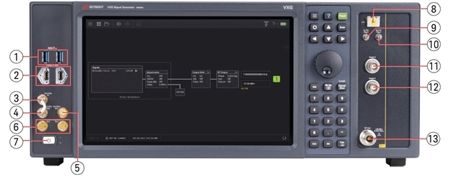
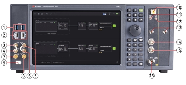
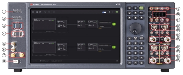
This topic describes the front and rear-panel connectors for the M9484C VXG.
For M9484C Option 001 and Option 506 or 508 only
|
Item |
Connector Type
|
Description
|
|
|
# |
Name |
||
|
1 |
SS - USB 3.0 |
USB Type-A female |
Host controller, SuperSpeed, 900 mA (nominal) |
|
2 |
USB-C PD |
USB Type-C female |
Reserved for future use. The front panel USB 3.0 Type C connectors do not have USB-compliant pin configurations. Do not use these ports for any USB devices as damage may occur. |
|
3 |
19.2 GHz Ina |
SMA |
19.2 GHz input 50 Ω impedance The power level range is 0-3 dBm. This range is nominal to minimize distortion and get the best signal fidelity. |
|
4 |
19.2 GHz Outa |
SMA |
Output of 19.2 GHz frequency reference. A factory installed cable connects the top left 19.2 GHz Out connector to the 19.2 GHz In. This port is always on. If unused, this port should be terminated with 50 Ω load. The power level range is 0-2 dBm. This range is nominal to minimize distortion and get the best signal fidelity. |
|
5 |
19.2 GHz Out |
SMA |
Output of 19.2 GHz frequency reference. The top right 19.2 GHz Out connector is switchable and off by default. The power level range is 0-2 dBm. This range is nominal to minimize distortion and get the best signal fidelity. |
|
6 |
19.2 GHz Out |
SMA |
Output of 19.2 GHz frequency reference. The two bottom 19.2 GHz Out connectors have a factory installed 50 Ω termination. This port is always on. If unused, this port should be terminated with 50 Ω load. The power level range is 0-2 dBm. This range is nominal to minimize distortion and get the best signal fidelity. |
|
7 |
On/Off Switch |
Push Button |
Power Switch. Refer to Power On/Standby (Instrument Shutdown). |
|
8 |
ODI |
ODI |
Optical Digital Interface. Optical interconnect for very high speed streaming applications between instruments, processors, and storage. |
|
9 |
Tx FC/Trig 2 |
SMB |
Dual function connector: ODI transmit flow control or trigger input/output 2. Input: 1.8 V LVCMOS 1 MΩ impedance Output: 1.8 V LVCMOS 50 Ω impedance (nominal) Damage level is outside of -0.5 V to 5.5 V |
|
10 |
Rx FC/Trig 3 |
SMB |
Dual function connector: ODI receive flow control or trigger input/output 3. Input: 1.8 V LVCMOS 1 MΩ impedance Output: 1.8 V LVCMOS 50 Ω impedance (nominal) Damage level is outside of -0.5 V to 5.5 V |
|
11 |
Event 2 |
BNC |
Baseband Marker Output #2 Maximum Edge Rate: every 1.667 ns VOL < 0.4 V, VOH is 2.8 V to 3.3 V into high impedance 50 Ω impedance (nominal) Damage level is outside of -0.5 V to 3.8 V |
|
12 |
Event 3 |
BNC |
Baseband Marker Output #3 Maximum Edge Rate: every 1.667 ns VOL < 0.4 V, VOH is 2.8 V to 3.3 V into high impedance 50 Ω impedance (nominal) Damage level is outside of -0.5 V to 3.8 V |
|
13 |
RF Out |
Type N female |
RF Output signal, level selected by user interface. 50 Ω impedance (nominal) +30 dBm Max reverse power, 0 VDC maximum |
The 2.4 GHz and 19.2 GHz input and output ports are designed for phase coherent operation between one or more M9484C VXG signal generators. Keysight Technologies recommends that you do not connect an external 2.4 GHz or 19.2 GHz signal to the M9484C VXG 2.4 GHz or 19.2 GHz inputs as the instrument specifications will not be covered by the warranty.
Jumper removal and connection should be performed when the VXG is powered off.
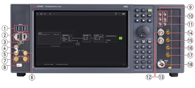
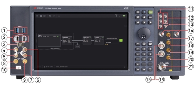
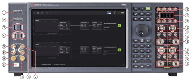
For M9484C Option 001, Option 506 or 508, and Option AN1
|
Item |
Connector Type
|
Description
|
|
|
# |
Name |
||
|
1 |
SS - USB 3.0 |
USB Type-A female |
Host controller, SuperSpeed, 900 mA (nominal) |
|
2 |
USB-C PD |
USB Type-C female |
Reserved for future use. The front panel USB 3.0 Type C connectors do not have USB-compliant pin configurations. Do not use these ports for any USB devices as damage may occur. |
|
3 |
Aux I/O |
Micro HDMI Type D |
Auxiliary Input/Output port 12 bit single-ended IOs 50 MHz maximum frequency (drive or receive) As a Driver: 3.3 V Output 5.5 V, 3.8 V when high or low state 50 Ω output resistance As a Receiver: 3.3 V output 5 V tolerant input (damage at 5.5 V) 10 k Ω input termination |
|
4 |
19.2 GHz Ina |
SMA |
19.2 GHz input 50 Ω impedance The power level range is 0-3 dBm. This range is nominal to minimize distortion and get the best signal fidelity. |
|
5 |
19.2 GHz Outa |
SMA |
Output of 19.2 GHz frequency reference. A factory installed cable connects the 19.2 GHz Out connector to the 19.2 GHz In. This port is always on. If unused, this port should be terminated with 50 Ω load. The power level range is 0-2 dBm. This range is nominal to minimize distortion and get the best signal fidelity. |
|
6 |
19.2 GHz Out |
SMA |
Output of 19.2 GHz frequency reference. The top right 19.2 GHz Out connector is switchable and off by default. The power level range is 0-2 dBm. This range is nominal to minimize distortion and get the best signal fidelity. |
|
7 |
19.2 GHz Out |
SMA |
Output of 19.2 GHz frequency reference. This 19.2 GHz Out connector has a factory installed 50 Ω termination. This port is always on. If unused, this port should be terminated with 50 Ω load. The power level range is 0-2 dBm. This range is nominal to minimize distortion and get the best signal fidelity. |
|
8 |
On/Off Switch |
Push Button |
Power Switch. Refer to Power On/Standby (Instrument Shutdown). |
|
9 |
Trig A, B, or C |
SMB |
General Purpose Trigger/Marker Ports 100 MHz maximum frequency (drive or receive) As a driver: 3.3 V output 5.5 V and 3.8 V when in high or low state 50 Ω output resistance As a receiver: 5 V input 5 V tolerant input (damage at 5.5 V) Selectable input termination (50 Ω or 10 K Ω) Receiver threshold resolution (5 mV) |
|
10 |
Ext 1 or 2 |
SMB |
External Inputs 1 and 2 16 bit ADC Selectable input impedance: 50 Ω, 600 Ω, or 1 M Ω Input Bandwidth: 10 MHz Input Range: ±1 V (±5 V tolerant) |
|
11 |
LF Out |
SMB |
Low Frequency Output 16 bit DAC Output impedance: 50 Ω (5 MHz to 10 MHz) Output range into 1 M Ω: ±6.5 V (DC to 5 MHz), ±4.5 V (5 MHz to 10 MHz) Bandwidth: 10 MHz (sine wave); 2 MHz (square and triangle waves) |
|
12 |
Event 2 |
BNC |
Baseband Marker Output #2 Maximum Edge Rate: every 1.667 ns VOL < 0.4 V, VOH is 2.8 V to 3.3 V into high impedance 50 Ω impedance (nominal) Damage level is outside of -0.5 V to 3.8 V |
|
13 |
Event 3 |
BNC |
Baseband Marker Output #3 Maximum Edge Rate: every 1.667 ns VOL < 0.4 V, VOH is 2.8 V to 3.3 V into high impedance 50 Ω impedance (nominal) Damage level is outside of -0.5 V to 3.8 V |
|
14 |
I+ Out |
SMA |
Analog In-phase component of I/Q modulation from channel 1's internal baseband generator. Frequency range is DC to 1000 MHz (nominal) 50 Ω impedance (nominal) Damage Level is ±2 V |
|
15 |
I- Out |
SMA |
Analog in-phase component of I/Q modulation from channel 1's internal baseband generator. Frequency range is DC to 1000 MHz (nominal) 50 Ω impedance (nominal) Damage Level is ±2 V |
|
16 |
Q+ Out |
SMA |
Analog quadrature-phase component of I/Q modulation from channel 1's internal baseband generator. Frequency range is DC to 1000 MHz (nominal) 50 Ω impedance (nominal) Damage Level is ±2 V |
|
17 |
Q- Out |
SMA |
Analog quadrature-phase component of I/Q modulation from channel 1's internal baseband generator. Frequency range is DC to 1000 MHz (nominal) 50 Ω impedance (nominal) Damage Level is ±2 V |
|
18 |
RF Out |
Type N Female |
RF Output signal, level selected by user interface. 50 Ω impedance (nominal) +30 dBm Max reverse power, 0 VDC maximum |
The 2.4 GHz and 19.2 GHz input and output ports are designed for phase coherent operation between one or more M9484C VXG signal generators. Keysight Technologies recommends that you do not connect an external 2.4 GHz or 19.2 GHz signal to the M9484C VXG 2.4 GHz or 19.2 GHz inputs as the instrument specifications will not be covered by the warranty.
Jumper removal and connection should be performed when the VXG is powered off.
For M9484C Option 001 and Option 514 or 520
|
Item |
Connector Type
|
Description
|
|
|
# |
Name |
||
|
1 |
SS - USB 3.0 |
USB Type-A female |
Host controller, SuperSpeed, 900 mA (nominal) |
|
2 |
USB-C PD |
USB Type-C female |
Reserved for future use. The front panel USB 3.0 Type C connectors do not have USB-compliant pin configurations. Do not use these ports for any USB devices as damage may occur. |
|
3 |
2.4 GHz Ina |
SMA |
2.4 GHz input 50 Ω impedance The power level range is 10-13 dBm (MAX). Hardware damage can occur if the power level exceeds the maximum value in this input range. |
|
4 |
2.4 GHz Outa |
SMA |
Output of 2.4 GHz frequency reference. A factory installed cable connects the 2.4 GHz Out connector to the 2.4 GHz In. This port is always on. If unused, this port should be terminated with 50 Ω load. The power level range is 11-13 dBm. This range is nominal to minimize distortion and get the best signal fidelity. |
|
5 |
19.2 GHz Ina |
SMA |
19.2 GHz input 50 Ω impedance The power level range is 0-3 dBm. This range is nominal to minimize distortion and get the best signal fidelity. |
|
6 |
19.2 GHz Outa |
SMA |
Output of 19.2 GHz frequency reference. A factory installed cable connects the 19.2 GHz Out connector to the 19.2 GHz In. This port is always on. If unused, this port should be terminated with 50 Ω load. The power level range is 0-2 dBm. This range is nominal to minimize distortion and get the best signal fidelity. |
|
7 |
2.4 GHz Out |
SMA |
Output of 2.4 GHz frequency reference. This 2.4 GHz Out connector has a factory installed 50 Ω termination. This port is always on. If unused, this port should be terminated with 50 Ω load. The power level range is 11-13 dBm. This range is nominal to minimize distortion and get the best signal fidelity. |
|
8 |
19.2 GHz Out |
SMA |
Output of 19.2 GHz frequency reference. This 19.2 GHz Out connector has a factory installed 50 Ω termination. This port is always on. If unused, this port should be terminated with 50 Ω load. The power level range is 0-2 dBm. This range is nominal to minimize distortion and get the best signal fidelity. |
|
9 |
On/Off Switch |
Push Button |
Power Switch. Refer to Power On/Standby (Instrument Shutdown). |
|
10 |
ODI |
ODI |
Optical Digital Interface. Optical interconnect for very high speed streaming applications between instruments, processors, and storage. |
|
11 |
Tx FC/Trig 2 |
SMB |
Dual function connector: ODI transmit flow control or trigger input/output 2 Input: 1.8 V LVCMOS 1 MΩ impedance Output: 1.8 V LVCMOS 50 Ω impedance (nominal) Damage level is outside of -0.5 V to 5.5 V |
|
12 |
Rx FC/Trig 3 |
SMB |
Dual function connector: ODI receive flow control or trigger input/output 3 Input: 1.8 V LVCMOS 1 MΩ impedance Output: 1.8 V LVCMOS 50 Ω impedance (nominal) Damage level is outside of -0.5 V to 5.5 V |
|
13 |
Event 2 |
BNC |
Baseband Marker Output #2 Maximum Edge Rate: every 1.667 ns VOL < 0.4 V, VOH is 2.8 V to 3.3 V into high impedance 50 Ω impedance (nominal) Damage level is outside of -0.5 V to 3.8 V |
|
14 |
Event 3 |
BNC |
Baseband Marker Output #3 Maximum Edge Rate: every 1.667 ns VOL < 0.4 V, VOH is 2.8 V to 3.3 V into high impedance 50 Ω impedance (nominal) Damage level is outside of -0.5 V to 3.8 V |
|
15 |
RF Out |
APC 3.5 mm |
RF Output signal, level selected by user interface. 50 Ω impedance (nominal) +30 dBm Max reverse power, 0 VDC maximum |
The 2.4 GHz and 19.2 GHz input and output ports are designed for phase coherent operation between one or more M9484C VXG signal generators. Keysight Technologies recommends that you do not connect an external 2.4 GHz or 19.2 GHz signal to the M9484C VXG 2.4 GHz or 19.2 GHz inputs as the instrument specifications will not be covered by the warranty.
Jumper removal and connection should be performed when the VXG is powered off.
For M9484C Option 001, Option 514 or 520, and Option AN1
|
Item |
Connector Type
|
Description
|
|
|
# |
Name |
||
|
1 |
SS - USB 3.0 |
USB Type-A female |
Host controller, SuperSpeed, 900 mA (nominal) |
|
2 |
USB-C PD |
USB Type-C female |
Reserved for future use. The front panel USB 3.0 Type C connectors do not have USB-compliant pin configurations. Do not use these ports for any USB devices as damage may occur. |
|
3 |
Aux I/O |
Micro HDMI Type D |
Auxiliary Input/Output port 12 bit single-ended IOs 50 MHz maximum frequency (drive or receive) As a Driver: 3.3 V Output 5.5 V, 3.8 V when high or low state 50 Ω output resistance As a Receiver: 3.3 V output 5 V tolerant input (damage at 5.5 V) 10 k Ω input termination |
|
4 |
2.4 GHz Ina |
SMA |
2.4 GHz input 50 Ω impedance The power level range is 10-13 dBm (MAX). Hardware damage can occur if the power level exceeds the maximum value in this input range. |
|
5 |
2.4 GHz Outa |
SMA |
Output of 2.4 GHz frequency reference. A factory installed cable connects the 2.4 GHz Out connector to the 2.4 GHz In. This port is always on. If unused, this port should be terminated with 50 Ω load. The power level range is 11-13 dBm. This range is nominal to minimize distortion and get the best signal fidelity. |
|
6 |
19.2 GHz Ina |
SMA |
19.2 GHz input 50 Ω impedance The power level range is 0-3 dBm. This range is nominal to minimize distortion and get the best signal fidelity. |
|
7 |
19.2 GHz Outa |
SMA |
Output of 19.2 GHz frequency reference. A factory installed cable connects the 19.2 GHz Out connector to the 19.2 GHz In. This port is always on. If unused, this port should be terminated with 50 Ω load. The power level range is 0-2 dBm. This range is nominal to minimize distortion and get the best signal fidelity. |
|
8 |
2.4 GHz Out |
SMA |
Output of 2.4 GHz frequency reference. This 2.4 GHz Out connector has a factory installed 50 Ω termination. This port is always on. If unused, this port should be terminated with 50 Ω load. The power level range is 11-13 dBm. This range is nominal to minimize distortion and get the best signal fidelity. |
|
9 |
19.2 GHz Out |
SMA |
Output of 19.2 GHz frequency reference. This 19.2 GHz Out connector has a factory installed 50 Ω termination. This port is always on. If unused, this port should be terminated with 50 Ω load. The power level range is 0-2 dBm. This range is nominal to minimize distortion and get the best signal fidelity. |
|
10 |
On/Off Switch |
Push Button |
Power Switch. Refer to Power On/Standby (Instrument Shutdown). |
|
11 |
Trig A, B or C |
SMB |
General Purpose Trigger/Marker Ports 100 MHz maximum frequency (drive or receive) As a driver: 3.3 V output 5.5 V and 3.8 V when in high or low state 50 Ω output resistance As a receiver: 5 V input 5 V tolerant input (damage at 5.5 V) Selectable input termination (50 Ω or 10 K Ω) Receiver threshold resolution (5 mV) |
|
12 |
Ext 1 or 2 |
SMB |
External Inputs 1 and 2 16 bit ADC Selectable input impedance: 50 Ω, 600 Ω, or 1 M Ω Input Bandwidth: 10 MHz Input Range: ±1 V (±5 V tolerant) |
|
13 |
LF Out |
SMB |
Low Frequency Output 16 bit DAC Output impedance: 50 Ω (5 MHz to 10 MHz) Output range into 1 M Ω: ±6.5 V (DC to 5 MHz), ±4.5 V (5 MHz to 10 MHz) Bandwidth: 10 MHz (sine wave); 2 MHz (square and triangle waves) |
|
14 |
Event 2 |
BNC |
Baseband Marker Output #2 Maximum Edge Rate: every 1.667 ns VOL < 0.4 V, VOH is 2.8 V to 3.3 V into high impedance 50 Ω impedance (nominal) Damage level is outside of -0.5 V to 3.8 V |
|
15 |
Event 3 |
BNC |
Baseband Marker Output #3 Maximum Edge Rate: every 1.667 ns VOL < 0.4 V, VOH is 2.8 V to 3.3 V into high impedance 50 Ω impedance (nominal) Damage level is outside of -0.5 V to 3.8 V |
|
16 |
I+ Out |
SMA |
Analog In-phase component of I/Q modulation from channel 1's internal baseband generator. Frequency range is DC to 1000 MHz (nominal) 50 Ω impedance (nominal) Damage Level is ±2 V |
|
17 |
I- Out |
SMA |
Analog in-phase component of I/Q modulation from channel 1's internal baseband generator. Frequency range is DC to 1000 MHz (nominal) 50 Ω impedance (nominal) Damage Level is ±2 V |
|
18 |
Q+ Out |
SMA |
Analog quadrature-phase component of I/Q modulation from channel 1's internal baseband generator. Frequency range is DC to 1000 MHz (nominal) 50 Ω impedance (nominal) Damage Level is ±2 V |
|
19 |
Q- Out |
SMA |
Analog quadrature-phase component of I/Q modulation from channel 1's internal baseband generator. Frequency range is DC to 1000 MHz (nominal) 50 Ω impedance (nominal) Damage Level is ±2 V |
|
20 |
RF Out |
APC 3.5 mm |
RF Output signal, level selected by user interface. 50 Ω impedance (nominal) +30 dBm max reverse power, 0 VDC maximum |
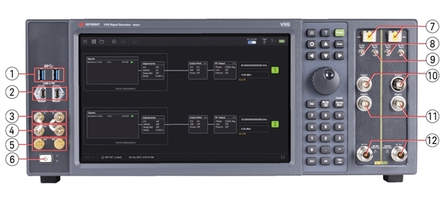
For M9484C Option 001 and Option 532 or 540 or 554
|
Item |
Connector Type
|
Description
|
|
|
# |
Name |
||
|
1 |
SS - USB 3.0 |
USB Type-A female |
Host controller, SuperSpeed, 900 mA (nominal) |
|
2 |
USB-C PD |
USB Type-C female |
USB 3.0 Type C. Provides power and digital control to the V3080A Vector Signal Generator Frequency Extender. The front panel USB 3.0 Type C connectors do not have USB-compliant pin configurations. Do not use these ports for any USB devices as damage may occur. |
|
3 |
2.4 GHz Ina |
SMA |
2.4 GHz input 50 Ω impedance The power level range is 11-17 dBm. This range is nominal to minimize distortion and get the best signal fidelity. |
|
4 |
2.4 GHz Outa |
SMA |
Output of 2.4 GHz frequency reference. A factory installed cable connects the 2.4 GHz Out connector to the 2.4 GHz In. This port is always on. If unused, this port should be terminated with 50 Ω load. The power level range is 15-17 dBm. This range is nominal to minimize distortion and get the best signal fidelity. |
|
5 |
19.2 GHz Ina |
SMA |
19.2 GHz input 50 Ω impedance The power level range is -2 to 7 dBm (MAX). Hardware damage can occur if the power level exceeds the maximum value in this input range. |
|
6 |
19.2 GHz Outa |
SMA |
Output of 19.2 GHz frequency reference. A factory installed cable connects the 19.2 GHz Out connector to the 19.2 GHz In. This port is always on. If unused, this port should be terminated with 50 Ω load. The power level range is -1 to 2 dBm. This range is nominal to minimize distortion and get the best signal fidelity. |
|
7 |
2.4 GHz Out |
SMA |
Output of 2.4 GHz frequency reference. This 2.4 GHz Out connector has a factory installed 50 Ω termination. This port is always on. If unused, this port should be terminated with 50 Ω load. The power level range is 15-17 dBm. This range is nominal to minimize distortion and get the best signal fidelity. |
|
8 |
19.2 GHz Out |
SMA |
Output of 19.2 GHz frequency reference. This 19.2 GHz Out connector has a factory installed 50 Ω termination. This port is always on. If unused, this port should be terminated with 50 Ω load. The power level range is -1 to 2 dBm. This range is nominal to minimize distortion and get the best signal fidelity. |
|
9 |
On/Off Switch |
Push Button |
Power Switch. Refer to Power On/Standby (Instrument Shutdown). |
|
10 |
ODI |
ODI |
Optical Digital Interface. Optical interconnect for very high speed streaming applications between instruments, processors, and storage. |
|
11 |
Tx FC/Trig 2 |
SMB |
Dual function connector: ODI transmit flow control or trigger input/output 2 Input: 1.8 V LVCMOS 1 MΩ impedance Output: 1.8 V LVCMOS 50 Ω impedance (nominal) Damage level is outside of -0.5 V to 5.5 V |
|
12 |
Rx FC/Trig 3 |
SMB |
Dual function connector: ODI receive flow control or trigger input/output 3 Input: 1.8 V LVCMOS 1 MΩ impedance Output: 1.8 V LVCMOS 50 Ω impedance (nominal) Damage level is outside of -0.5 V to 5.5 V |
|
13 |
LO1 and LO2 |
APC 3.5 mm |
9.6 GHz signal |
|
14 |
Event 2 |
BNC |
Baseband Marker Output #2 Maximum Edge Rate: every 1.667 ns VOL < 0.4 V, VOH is 2.8 V to 3.3 V into high impedance 50 Ω impedance (nominal) Damage level is outside of -0.5 V to 3.8 V |
|
15 |
Event 3 |
BNC |
Baseband Marker Output #3 Maximum Edge Rate: every 1.667 ns VOL < 0.4 V, VOH is 2.8 V to 3.3 V into high impedance 50 Ω impedance (nominal) Damage level is outside of -0.5 V to 3.8 V |
|
16 |
RF Out |
1.85 mm |
RF Output signal, level selected by user interface. 50 Ω impedance (nominal) +24 dBm maximum reverse power, 0 VDC Max |
The 2.4 GHz and 19.2 GHz input and output ports are designed for phase coherent operation between one or more M9484C VXG signal generators. Keysight Technologies recommends that you do not connect an external 2.4 GHz or 19.2 GHz signal to the M9484C VXG 2.4 GHz or 19.2 GHz inputs as the instrument specifications will not be covered by the warranty.
Jumper removal and connection should be performed when the VXG is powered off.
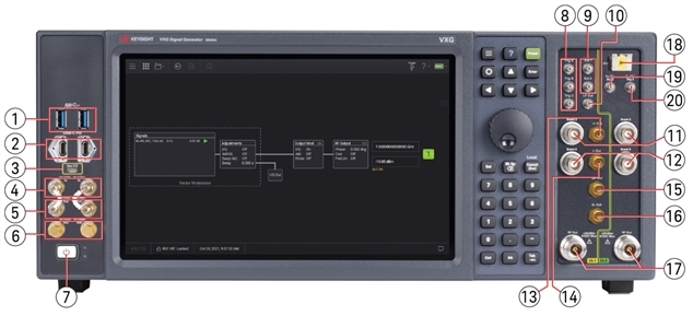
For M9484C Option 001, Option 532 or 540 or 554, and Option AN1
|
Item |
Connector Type
|
Description
|
|
|
# |
Name |
||
|
1 |
SS - USB 3.0 |
USB Type-A female |
Host controller, SuperSpeed, 900 mA (nominal) |
|
2 |
USB-C PD |
USB Type-C female |
USB 3.0 Type C. Provides power and digital control to the V3080A Vector Signal Generator Frequency Extender. The front panel USB 3.0 Type C connectors do not have USB-compliant pin configurations. Do not use these ports for any USB devices as damage may occur. |
|
3 |
Aux I/O |
|
Auxiliary Input/Output port 12 bit single-ended IOs 50 MHz maximum frequency (drive or receive) As a Driver: 3.3 V Output 5.5 V, 3.8 V when high or low state 50 Ω output resistance As a Receiver: 3.3 V output 5 V tolerant input (damage at 5.5 V) 10 k Ω input termination |
|
4 |
2.4 GHz Ina |
SMA |
2.4 GHz input 50 Ω impedance The power level range is 11-17 dBm. This range is nominal to minimize distortion and get the best signal fidelity. |
|
5 |
2.4 GHz Outa |
SMA |
Output of 2.4 GHz frequency reference. A factory installed cable connects the 2.4 GHz Out connector to the 2.4 GHz In. This port is always on. If unused, this port should be terminated with 50 Ω load. The power level range is 15-17 dBm. This range is nominal to minimize distortion and get the best signal fidelity. |
|
6 |
19.2 GHz Ina |
SMA |
19.2 GHz input 50 Ω impedance The power level range is -2 to 7 dBm (MAX). Hardware damage can occur if the power level exceeds the maximum value in this input range. |
|
7 |
19.2 GHz Outa |
SMA |
Output of 19.2 GHz frequency reference. A factory installed cable connects the 19.2 GHz Out connector to the 19.2 GHz In. This port is always on. If unused, this port should be terminated with 50 Ω load. The power level range is -1 to 2 dBm. This range is nominal to minimize distortion and get the best signal fidelity. |
|
8 |
2.4 GHz Out |
SMA |
Output of 2.4 GHz frequency reference. This 2.4 GHz Out connector has a factory installed 50 Ω termination. This port is always on. If unused, this port should be terminated with 50 Ω load. The power level range is 15-17 dBm. This range is nominal to minimize distortion and get the best signal fidelity. |
|
9 |
19.2 GHz Out |
SMA |
Output of 19.2 GHz frequency reference. This 19.2 GHz Out connector has a factory installed 50 Ω termination. This port is always on. If unused, this port should be terminated with 50 Ω load. The power level range is -1 to 2 dBm. This range is nominal to minimize distortion and get the best signal fidelity. |
|
10 |
On/Off Switch |
Push Button |
Power Switch. Refer to Power On/Standby (Instrument Shutdown). |
|
11 |
Trig A, B or C |
SMB |
General Purpose Trigger/Marker Ports 100 MHz maximum frequency (drive or receive) As a driver: 3.3 V output 5.5 V and 3.8 V when in high or low state 50 Ω output resistance As a receiver: 5 V input 5 V tolerant input (damage at 5.5 V) Selectable input termination (50 Ω or 10 K Ω) Receiver threshold resolution (5 mV) |
|
12 |
Ext 1 or 2 |
SMB |
External Inputs 1 and 2 16 bit ADC Selectable input impedance: 50 Ω, 600 Ω, or 1 M Ω Input Bandwidth: 10 MHz Input Range: ±1 V (±5 V tolerant) |
|
13 |
LF Out |
SMB |
Low Frequency Output 16 bit DAC Output impedance: 50 Ω (5 MHz to 10 MHz) Output range into 1 M Ω: ±6.5 V (DC to 5 MHz), ±4.5 V (5 MHz to 10 MHz) Bandwidth: 10 MHz (sine wave); 2 MHz (square and triangle waves) |
|
14 |
LO 1 and LO 2 |
APC 3.5 mm |
9.6 GHz signal |
|
15 |
Event 2 |
BNC |
Baseband Marker Output #2 Maximum Edge Rate: every 1.667 ns VOL < 0.4 V, VOH is 2.8 V to 3.3 V into high impedance 50 Ω impedance (nominal) Damage level is outside of -0.5 V to 3.8 V |
|
16 |
Event 3 |
BNC |
Baseband Marker Output #3 Maximum Edge Rate: every 1.667 ns VOL < 0.4 V, VOH is 2.8 V to 3.3 V into high impedance 50 Ω impedance (nominal) Damage level is outside of -0.5 V to 3.8 V |
|
17 |
I+ Out |
SMA |
Analog In-phase component of I/Q modulation from channel 1's internal baseband generator. Frequency range is DC to 1000 MHz (nominal) 50 Ω impedance (nominal) Damage Level is ±2 V |
|
18 |
I- Out |
SMA |
Analog in-phase component of I/Q modulation from channel 1's internal baseband generator. Frequency range is DC to 1000 MHz (nominal) 50 Ω impedance (nominal) Damage Level is ±2 V |
|
19 |
Q+ Out |
SMA |
Analog quadrature-phase component of I/Q modulation from channel 1's internal baseband generator. Frequency range is DC to 1000 MHz (nominal) 50 Ω impedance (nominal) Damage Level is ±2 V |
|
20 |
Q- Out |
SMA |
Analog quadrature-phase component of I/Q modulation from channel 1's internal baseband generator. Frequency range is DC to 1000 MHz (nominal) 50 Ω impedance (nominal) Damage Level is ±2 V |
|
21 |
RF Out |
1.85 mm |
RF Output signal, level selected by user interface. 50 Ω impedance (nominal) +24 dBm maximum reverse power, 0 VDC Max |
The 2.4 GHz and 19.2 GHz input and output ports are designed for phase coherent operation between one or more M9484C VXG signal generators. Keysight Technologies recommends that you do not connect an external 2.4 GHz or 19.2 GHz signal to the M9484C VXG 2.4 GHz or 19.2 GHz inputs as the instrument specifications will not be covered by the warranty.
Jumper removal and connection should be performed when the VXG is powered off.
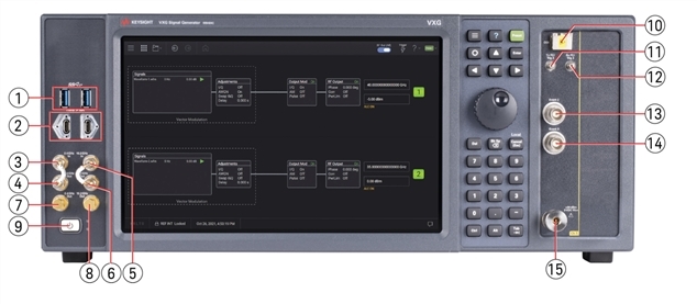
For M9484C Option 001 + 002 and 506 or 508
|
Item |
Connector Type
|
Description
|
|
|
# |
Name |
||
|
1 |
SS - USB 3.0 |
USB Type-A female |
Host controller, SuperSpeed, 900 mA (nominal) |
|
2 |
USB-C PD |
USB Type-C female |
Reserved for future use. The front panel USB 3.0 Type C connectors do not have USB-compliant pin configurations. Do not use these ports for any USB devices as damage may occur. |
|
3 |
19.2 GHz Ina |
SMA |
19.2 GHz input 50 Ω impedance The power level range is 0-3 dBm. This range is nominal to minimize distortion and get the best signal fidelity. |
|
4 |
19.2 GHz Outa |
SMA |
Output of 19.2 GHz frequency reference. A factory installed cable connects the 19.2 GHz Out connector to the 19.2 GHz In. This port is always on. If unused, this port should be terminated with 50 Ω load. The power level range is 0-2 dBm. This range is nominal to minimize distortion and get the best signal fidelity. |
|
5 |
19.2 GHz Out |
SMA |
Output of 19.2 GHz frequency reference. These two 19.2 GHz Out connectors have a factory installed 50 Ω termination. This port is always on. If unused, this port should be terminated with 50 Ω load. The power level range is 0-2 dBm. This range is nominal to minimize distortion and get the best signal fidelity. |
|
6 |
On/Off Switch |
Push Button |
Power Switch. Refer to Power On/Standby (Instrument Shutdown). |
|
7 |
ODI |
ODI |
Optical Digital Interface. Optical interconnect for very high speed streaming applications between instruments, processors, and storage. |
|
8 |
Tx FC/Trig 2 |
SMB |
Dual function connector: ODI transmit flow control or trigger input/output 2 Input: 1.8 V LVCMOS 1 MΩ impedance Output: 1.8 V LVCMOS 50 Ω impedance (nominal) Damage level is outside of -0.5 V to 5.5 V |
|
9 |
Rx FC/Trig 3 |
SMB |
Dual function connector: ODI receive flow control or trigger input/output 3 Input: 1.8 V LVCMOS 1 MΩ impedance Output: 1.8 V LVCMOS 50 Ω impedance (nominal) Damage level is outside of -0.5 V to 5.5 V |
|
10 |
Event 2 |
BNC |
Baseband Marker Output #2 Maximum Edge Rate: every 1.667 ns VOL < 0.4 V, VOH is 2.8 V to 3.3 V into high impedance 50 Ω impedance (nominal) Damage level is outside of -0.5 V to 3.8 V |
|
11 |
Event 3 |
BNC |
Baseband Marker Output #3 Maximum Edge Rate: every 1.667 ns VOL < 0.4 V, VOH is 2.8 V to 3.3 V into high impedance 50 Ω impedance (nominal) Damage level is outside of -0.5 V to 3.8 V |
|
12 |
RF Out |
Type N female |
RF Output signal, level selected by user interface. 50 Ω impedance (nominal) +30 dBm max reverse power, 0 VDC maximum |
The 2.4 GHz and 19.2 GHz input and output ports are designed for phase coherent operation between one or more M9484C VXG signal generators. Keysight Technologies recommends that you do not connect an external 2.4 GHz or 19.2 GHz signal to the M9484C VXG 2.4 GHz or 19.2 GHz inputs as the instrument specifications will not be covered by the warranty.
Jumper removal and connection should be performed when the VXG is powered off.
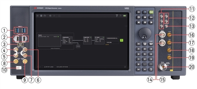
For M9484C Option 001 + 002, Option 506 or 508, and Option AN1
|
Item |
Connector Type
|
Description
|
|
|
# |
Name |
||
|
1 |
SS - USB 3.0 |
USB Type-A female |
Host controller, SuperSpeed, 900 mA (nominal) |
|
2 |
USB-C PD |
USB Type-C female |
Reserved for future use. The front panel USB 3.0 Type C connectors do not have USB-compliant pin configurations. Do not use these ports for any USB devices as damage may occur. |
|
3 |
Aux I/O |
Micro HDMI Type D |
Auxiliary Input/Output port 12 bit single-ended IOs 50 MHz maximum frequency (drive or receive) As a Driver: 3.3 V Output 5.5 V, 3.8 V when high or low state 50 Ω output resistance As a Receiver: 3.3 V output 5 V tolerant input (damage at 5.5 V) 10 k Ω input termination |
|
4 |
19.2 GHz Ina |
SMA |
19.2 GHz input 50 Ω impedance The power level range is 0-3 dBm. This range is nominal to minimize distortion and get the best signal fidelity. |
|
5 |
19.2 GHz Outa |
SMA |
Output of 19.2 GHz frequency reference. A factory installed cable connects the 19.2 GHz Out connector to the 19.2 GHz In. This port is always on. If unused, this port should be terminated with 50 Ω load. The power level range is 0-2 dBm. This range is nominal to minimize distortion and get the best signal fidelity. |
|
6 |
19.2 GHz Out |
SMA |
Output of 19.2 GHz frequency reference. This 19.2 GHz Out connector has a factory installed 50 Ω termination. This port is always on. If unused, this port should be terminated with 50 Ω load. The power level range is 0-2 dBm. This range is nominal to minimize distortion and get the best signal fidelity. |
|
7 |
On/Off Switch |
Push Button |
Power Switch. Refer to Power On/Standby (Instrument Shutdown). |
|
8 |
Trig A, B, or C |
SMB |
General Purpose Trigger/Marker Ports 100 MHz maximum frequency (drive or receive) As a Driver: 3.3 V output 5.5 V and 3.8 V when in high or low state 50 Ω output resistance As a Receiver: 5 V input 5 V tolerant input (damage at 5.5 V) Selectable input termination (50 Ω or 10 K Ω) Receiver threshold resolution (5 mV) |
|
9 |
Ext 1 or 2 |
SMB |
External Inputs 1 and 2 16 bit ADC Selectable input impedance: 50 Ω, 600 Ω, or 1 M Ω) Input Bandwidth: 10 MHz Input Range: ±1 V (±5 V tolerant) |
|
10 |
LF Out |
SMB |
Low Frequency Output 16 bit DAC Output impedance: 50 Ω (5 MHz to 10 MHz) Output range into 1 M Ω: ±6.5 V (DC to 5 MHz), ±4.5 V (5 MHz to 10 MHz) Bandwidth: 10 MHz (sine wave); 2 MHz (square and triangle waves) |
|
11 |
Event 2 |
BNC |
Baseband Marker Output #2 Maximum Edge Rate: every 1.667 ns VOL < 0.4 V, VOH is 2.8 V to 3.3 V into high impedance 50 Ω impedance (nominal) Damage level is outside of -0.5 V to 3.8 V |
|
12 |
Event 3 |
BNC |
Baseband Marker Output #3 Maximum Edge Rate: every 1.667 ns VOL < 0.4 V, VOH is 2.8 V to 3.3 V into high impedance 50 Ω impedance (nominal) Damage level is outside of -0.5 V to 3.8 V |
|
13 |
I+ Out |
SMA |
Analog In-phase component of I/Q modulation from channel 1's internal baseband generator. Frequency range is DC to 1000 MHz (nominal) 50 Ω impedance (nominal) Damage Level is ±2 V |
|
14 |
I- Out |
SMA |
Analog in-phase component of I/Q modulation from channel 1's internal baseband generator. Frequency range is DC to 1000 MHz (nominal) 50 Ω impedance (nominal) Damage Level is ±2 V |
|
15 |
Q+ Out |
SMA |
Analog quadrature-phase component of I/Q modulation from channel 1's internal baseband generator. Frequency range is DC to 1000 MHz (nominal) 50 Ω impedance (nominal) Damage Level is ±2 V |
|
16 |
Q- Out |
SMA |
Analog quadrature-phase component of I/Q modulation from channel 1's internal baseband generator. Frequency range is DC to 1000 MHz (nominal) 50 Ω impedance (nominal) Damage Level is ±2 V |
|
17 |
CH 1 and CH 2 RF Out |
Type N Female |
RF Output signal, level selected by user interface. 50 Ω impedance (nominal) +30 dBm, 0 VDC maximum |
|
18 |
ODI |
ODI |
Optical Digital Interface. Optical interconnect for very high speed streaming applications between instruments, processors, and storage. |
|
19 |
Tx FC/Trig 2 |
SMB |
Dual function connector: ODI transmit flow control or trigger input/output 2 Input: 1.8 V LVCMOS 1 MΩ impedance Output: 1.8 V LVCMOS 50 Ω impedance (nominal) Damage level is outside of -0.5 V to 5.5 V |
|
20 |
Rx FC/Trig 3 |
SMB |
Dual function connector: ODI receive flow control or trigger input/output 3 Input: 1.8 V LVCMOS 1 MΩ impedance Output: 1.8 V LVCMOS 50 Ω impedance (nominal) Damage level is outside of -0.5 V to 5.5 V |
The 2.4 GHz and 19.2 GHz input and output ports are designed for phase coherent operation between one or more M9484C VXG signal generators. Keysight Technologies recommends that you do not connect an external 2.4 GHz or 19.2 GHz signal to the M9484C VXG 2.4 GHz or 19.2 GHz inputs as the instrument specifications will not be covered by the warranty.
Jumper removal and connection should be performed when the VXG is powered off.
For M9484C Option 001 + 002 and 514 or 520
|
Item |
Connector Type
|
Description
|
|
|
# |
Name |
||
|
1 |
SS - USB 3.0 |
USB Type-A female |
Host controller, SuperSpeed, 900 mA (nominal) |
|
2 |
USB-C PD |
USB Type-C female |
Reserved for future use. The front panel USB 3.0 Type C connectors do not have USB-compliant pin configurations. Do not use these ports for any USB devices as damage may occur. |
|
3 |
2.4 GHz Ina |
SMA |
2.4 GHz input 50 Ω impedance The power level range is 11-17 dBm. This range is nominal to minimize distortion and get the best signal fidelity. |
|
4 |
2.4 GHz Outa |
SMA |
Output of 2.4 GHz frequency reference. A factory installed cable connects the 2.4 GHz Out connector to the 2.4 GHz In. This port is always on. If unused, this port should be terminated with 50 Ω load. The power level range is 15-17 dBm. This range is nominal to minimize distortion and get the best signal fidelity. |
|
5 |
19.2 GHz Ina |
SMA |
19.2 GHz input 50 Ω impedance The power level range is -2 to 7 dBm (MAX). Hardware damage can occur if the power level exceeds the maximum value in this input range. |
|
6 |
19.2 GHz Outa |
SMA |
Output of 19.2 GHz frequency reference. A factory installed cable connects the 19.2 GHz Out connector to the 19.2 GHz In. This port is always on. If unused, this port should be terminated with 50 Ω load. The power level range is -1 to 2 dBm. This range is nominal to minimize distortion and get the best signal fidelity. |
|
7 |
2.4 GHz Out |
SMA |
Output of 2.4 GHz frequency reference. This 2.4 GHz Out connector has a factory installed 50 Ω termination. This port is always on. If unused, this port should be terminated with 50 Ω load. The power level range is 11-13 dBm. This range is nominal to minimize distortion and get the best signal fidelity. |
|
8 |
19.2 GHz Out |
SMA |
Output of 19.2 GHz frequency reference. This 19.2 GHz Out connector has a factory installed 50 Ω termination. This port is always on. If unused, this port should be terminated with 50 Ω load. The power level range is 0-2 dBm. This range is nominal to minimize distortion and get the best signal fidelity. |
|
9 |
On/Off Switch |
Push Button |
Power Switch. Refer to Power On/Standby (Instrument Shutdown). |
|
10 |
ODI |
ODI |
Optical Digital Interface. Optical interconnect for very high speed streaming applications between instruments, processors, and storage. |
|
11 |
Tx FC/Trig 2 |
SMB |
Dual function connector: ODI transmit flow control or trigger input/output 2 Input: 1.8 V LVCMOS 1 MΩ impedance Output: 1.8 V LVCMOS 50 Ω impedance (nominal) Damage level is outside of -0.5 V to 5.5 V |
|
12 |
Rx FC/Trig 3 |
SMB |
Dual function connector: ODI receive flow control or trigger input/output 3 Input: 1.8 V LVCMOS 1 MΩ impedance Output: 1.8 V LVCMOS 50 Ω impedance (nominal) Damage level is outside of -0.5 V to 5.5 V |
|
13 |
Event 2 |
BNC |
Baseband Marker Output #2 Maximum Edge Rate: every 1.667 ns VOL < 0.4 V, VOH is 2.8 V to 3.3 V into high impedance 50 Ω impedance (nominal) Damage level is outside of -0.5 V to 3.8 V |
|
14 |
Event 3 |
BNC |
Baseband Marker Output #3 Maximum Edge Rate: every 1.667 ns VOL < 0.4 V, VOH is 2.8 V to 3.3 V into high impedance 50 Ω impedance (nominal) Damage level is outside of -0.5 V to 3.8 V |
|
15 |
RF Out |
APC 3.5 mm |
RF Output signal, level selected by user interface. 50 Ω impedance (nominal) +30 dBm max reverse power, 0 VDC maximum |
The 2.4 GHz and 19.2 GHz input and output ports are designed for phase coherent operation between one or more M9484C VXG signal generators. Keysight Technologies recommends that you do not connect an external 2.4 GHz or 19.2 GHz signal to the M9484C VXG 2.4 GHz or 19.2 GHz inputs as the instrument specifications will not be covered by the warranty.
Jumper removal and connection should be performed when the VXG is powered off.
For M9484C Option 001 + 002, 514 or 520, and AN1
|
Item |
Connector Type
|
Description
|
|
|
# |
Name |
||
|
1 |
SS - USB 3.0 |
USB Type-A female |
Host controller, SuperSpeed, 900 mA (nominal) |
|
2 |
USB-C PD |
USB Type-C female |
Reserved for future use. The front panel USB 3.0 Type C connectors do not have USB-compliant pin configurations. Do not use these ports for any USB devices as damage may occur. |
|
3 |
Aux I/O |
Micro HDMI Type D |
Auxiliary Input/Output port 12 bit single-ended IOs 50 MHz maximum frequency (drive or receive) As a Driver: 3.3 V Output 5.5 V, 3.8 V when high or low state 50 Ω output resistance As a Receiver: 3.3 V output 5 V tolerant input (damage at 5.5 V) 10 k Ω input termination |
|
4 |
2.4 GHz Ina |
SMA |
2.4 GHz input 50 Ω impedance The power level range is 11-17 dBm. This range is nominal to minimize distortion and get the best signal fidelity. |
|
5 |
2.4 GHz Outa |
SMA |
Output of 2.4 GHz frequency reference. A factory installed cable connects the 2.4 GHz Out connector to the 2.4 GHz In. This port is always on. If unused, this port should be terminated with 50 Ω load. The power level range is 15-17 dBm. This range is nominal to minimize distortion and get the best signal fidelity. |
|
6 |
19.2 GHz Ina |
SMA |
19.2 GHz input 50 Ω impedance The power level range is -2 to 7 dBm (MAX). Hardware damage can occur if the power level exceeds the maximum value in this input range. |
|
7 |
19.2 GHz Outa |
SMA |
Output of 19.2 GHz frequency reference. A factory installed cable connects the 19.2 GHz Out connector to the 19.2 GHz In. This port is always on. If unused, this port should be terminated with 50 Ω load. The power level range is -1 to 2 dBm. This range is nominal to minimize distortion and get the best signal fidelity. |
|
8 |
2.4 GHz Out |
SMA |
Output of 2.4 GHz frequency reference. This 2.4 GHz Out connector has a factory installed 50 Ω termination. This port is always on. If unused, this port should be terminated with 50 Ω load. The power level range is 11-13 dBm. This range is nominal to minimize distortion and get the best signal fidelity. |
|
9 |
19.2 GHz Out |
SMA |
Output of 19.2 GHz frequency reference. This 19.2 GHz Out connector has a factory installed 50 Ω termination. This port is always on. If unused, this port should be terminated with 50 Ω load. The power level range is 0-2 dBm. This range is nominal to minimize distortion and get the best signal fidelity. |
|
10 |
On/Off Switch |
Push Button |
Power Switch. Refer to Power On/Standby (Instrument Shutdown). |
|
11 |
Trig A, B, or C |
SMB |
General Purpose Trigger/Marker Ports 100 MHz maximum frequency (drive or receive) As a driver: 3.3 V output 5.5 V and 3.8 V when in high or low state 50 Ω output resistance As a receiver: 5 V input 5 V tolerant input (damage at 5.5 V) Selectable input termination (50 Ω or 10 K Ω) Receiver threshold resolution (5 mV) |
|
12 |
Ext 1 or 2 |
SMB |
External Inputs 1 and 2 16 bit ADC Selectable input impedance: 50 Ω, 600 Ω, or 1 M Ω Input Bandwidth: 10 MHz Input Range: ±1 V (±5 V tolerant) |
|
13 |
LF Out |
SMB |
Low Frequency Output 16 bit DAC Output impedance: 50 Ω (5 MHz to 10 MHz) Output range into 1 M Ω: ±6.5 V (DC to 5 MHz), ±4.5 V (5 MHz to 10 MHz) Bandwidth: 10 MHz (sine wave); 2 MHz (square and triangle waves) |
|
14 |
Event 2 |
BNC |
Baseband Marker Output #2 Maximum Edge Rate: every 1.667 ns VOL < 0.4 V, VOH is 2.8 V to 3.3 V into high impedance 50 Ω impedance (nominal) Damage level is outside of -0.5 V to 3.8 V |
|
15 |
Event 3 |
BNC |
Baseband Marker Output #3 Maximum Edge Rate: every 1.667 ns VOL < 0.4 V, VOH is 2.8 V to 3.3 V into high impedance 50 Ω impedance (nominal) Damage level is outside of -0.5 V to 3.8 V |
|
16 |
I+ Out |
SMA |
Analog In-phase component of I/Q modulation from channel 1's internal baseband generator. Frequency range is DC to 1000 MHz (nominal) 50 Ω impedance (nominal) Damage Level is ±2 V |
|
17 |
I- Out |
SMA |
Analog in-phase component of I/Q modulation from channel 1's internal baseband generator. Frequency range is DC to 1000 MHz (nominal) 50 Ω impedance (nominal) Damage Level is ±2 V |
|
18 |
Q+ Out |
SMA |
Analog quadrature-phase component of I/Q modulation from channel 1's internal baseband generator. Frequency range is DC to 1000 MHz (nominal) 50 Ω impedance (nominal) Damage Level is ±2 V |
|
19 |
Q- Out |
SMA |
Analog quadrature-phase component of I/Q modulation from channel 1's internal baseband generator. Frequency range is DC to 1000 MHz (nominal) 50 Ω impedance (nominal) Damage Level is ±2 V |
|
20 |
CH 1 or CH 2 RF Out |
APC 3.5 mm |
RF Output signal, level selected by user interface. 50 Ω impedance (nominal) +30 dBm max reverse power, 0 VDC maximum |
|
21 |
ODI |
ODI |
Optical Digital Interface. Optical interconnect for very high speed streaming applications between instruments, processors, and storage. |
|
22 |
Tx FC/Trig 2 |
SMB |
Dual function connector: ODI transmit flow control or trigger input/output 2 Input: 1.8 V LVCMOS 1 MΩ impedance Output: 1.8 V LVCMOS 50 Ω impedance (nominal) Damage level is outside of -0.5 V to 5.5 V |
|
23 |
Rx FC/Trig 3 |
SMB |
Dual function connector: ODI transmit flow control or trigger input/output 2 Input: 1.8 V LVCMOS 1 MΩ impedance Output: 1.8 V LVCMOS 50 Ω impedance (nominal) Damage level is outside of -0.5 V to 5.5 V |
The 2.4 GHz and 19.2 GHz input and output ports are designed for phase coherent operation between one or more M9484C VXG signal generators. Keysight Technologies recommends that you do not connect an external 2.4 GHz or 19.2 GHz signal to the M9484C VXG 2.4 GHz or 19.2 GHz inputs as the instrument specifications will not be covered by the warranty.
Jumper removal and connection should be performed when the VXG is powered off.
For M9484C Option 001 + 002, Option 532 or 544 or 554
|
Item |
Connector Type
|
Description
|
|
|
# |
Name |
||
|
1 |
System Sync Up |
|
Reserved for future use |
|
2 |
System Sync Down |
|
Reserved for future use |
|
3 |
SS - USB 3.0 |
USB Type-A female |
Host controller, SuperSpeed, 900 mA (nominal) |
|
4 |
USB-C PD |
USB Type-C female |
USB 3.0 Type C. Provides power and digital control to the V3080A Vector Signal Generator Frequency Extender. The front panel USB 3.0 Type C connectors do not have USB-compliant pin configurations. Do not use these ports for any USB devices as damage may occur. |
|
5 |
2.4 GHz Ina |
SMA |
2.4 GHz input 50 Ω impedance The power level range is 11-17 dBm. This range is nominal to minimize distortion and get the best signal fidelity. |
|
6 |
2.4 GHz Outa |
SMA |
Output of 2.4 GHz frequency reference. A factory installed cable connects the 2.4 GHz Out connector to the 2.4 GHz In. This port is always on. If unused, this port should be terminated with 50 Ω load. The power level range is 15-17 dBm. This range is nominal to minimize distortion and get the best signal fidelity. |
|
7 |
19.2 GHz Ina |
SMA |
19.2 GHz input 50 Ω impedance The power level range is -2 to 7 dBm (MAX). Hardware damage can occur if the power level exceeds the maximum value in this input range. |
|
8 |
19.2 GHz Outa |
SMA |
Output of 19.2 GHz frequency reference. A factory installed cable connects the 19.2 GHz Out connector to the 19.2 GHz In. This port is always on. If unused, this port should be terminated with 50 Ω load. The power level range is -1 to 2 dBm. This range is nominal to minimize distortion and get the best signal fidelity. |
|
9 |
2.4 GHz Out |
SMA |
Output of 2.4 GHz frequency reference. This 2.4 GHz Out connector has a factory installed 50 Ω termination. This port is always on. If unused, this port should be terminated with 50 Ω load. The power level range is 15-17 dBm. This range is nominal to minimize distortion and get the best signal fidelity. |
|
10 |
19.2 GHz Out |
SMA |
Output of 19.2 GHz frequency reference. This 19.2 GHz Out connector has a factory installed 50 Ω termination. This port is always on. If unused, this port should be terminated with 50 Ω load. The power level range is -1 to 2 dBm. This range is nominal to minimize distortion and get the best signal fidelity. |
|
11 |
On/Off Switch |
Push Button |
Power Switch. Refer to Power On/Standby (Instrument Shutdown). |
|
12 |
ODI |
ODI |
Optical Digital Interface. Optical interconnect for very high speed streaming applications between instruments, processors, and storage. |
|
13 |
Tx FC/Trig 2 |
SMB |
Dual function connector: ODI transmit flow control or trigger input/output 2 Input: 1.8 V LVCMOS 1 MΩ impedance Output: 1.8 V LVCMOS 50 Ω impedance (nominal) Damage level is outside of -0.5 V to 5.5 V |
|
14 |
Tx FC/Trig 3 |
SMB |
Dual function connector: ODI transmit flow control or trigger input/output 2 Input: 1.8 V LVCMOS 1 M Ω impedance Output: 1.8 V LVCMOS 50 Ω impedance (nominal) Damage level is outside of -0.5 V to 5.5 V |
|
15 |
LO 1 and LO 2 |
APC 3.5 mm |
9.6 GHz signal |
|
16 |
Event 2 |
BNC |
Baseband Marker Output #2 Maximum Edge Rate: every 1.667 ns VOL < 0.4 V, VOH is 2.8 V to 3.3 V into high impedance 50 Ω impedance (nominal) Damage level is outside of -0.5 V to 3.8 V |
|
17 |
Event 3 |
BNC |
Baseband Marker Output #3 Maximum Edge Rate: every 1.667 ns VOL < 0.4 V, VOH is 2.8 V to 3.3 V into high impedance 50 Ω impedance (nominal) Damage level is outside of -0.5 V to 3.8 V |
|
18 |
CH 1 and CH2 RF Out |
1.85 mm |
RF Output signal, level selected by user interface. 50 Ω impedance (nominal) +24 dBm maximum reverse power, 0 VDC |
The 2.4 GHz and 19.2 GHz input and output ports are designed for phase coherent operation between one or more M9484C VXG signal generators. Keysight Technologies recommends that you do not connect an external 2.4 GHz or 19.2 GHz signal to the M9484C VXG 2.4 GHz or 19.2 GHz inputs as the instrument specifications will not be covered by the warranty.
Jumper removal and connection should be performed when the VXG is powered off.
For M9484C Option 001 + 002, Option 532 or 544 or 554, and Option AN1
|
Item |
Connector Type
|
Description
|
|
|
# |
Name |
||
|
1 |
System Sync Up |
|
Reserved for future use |
|
2 |
System Sync Down |
|
Reserved for future use |
|
3 |
SS - USB 3.0 |
USB Type-A female |
Host controller, SuperSpeed, 900 mA (nominal) |
|
4 |
USB-C PD |
USB Type-C female |
USB 3.0 Type C. Provides power and digital control to the V3080A Vector Signal Generator Frequency Extender. The front panel USB 3.0 Type C connectors do not have USB-compliant pin configurations. Do not use these ports for any USB devices as damage may occur. |
|
5 |
Aux I/O |
Micro HDMI Type D |
Auxiliary Input/Output port 12 bit single-ended IOs 50 MHz maximum frequency (drive or receive) As a Driver: 3.3 V Output 5.5 V, 3.8 V when high or low state 50 Ω output resistance As a Receiver: 3.3 V output 5 V tolerant input (damage at 5.5 V) 10 k Ω input termination |
|
6 |
2.4 GHz Ina |
SMA |
2.4 GHz input 50 Ω impedance The power level range is 11-17 dBm. Damage can occur if the power level exceeds the maximum value in this range. |
|
7 |
2.4 GHz Outa |
SMA |
Output of 2.4 GHz frequency reference. A factory installed cable connects the 2.4 GHz Out connector to the 2.4 GHz In. This port is always on. If unused, this port should be terminated with 50 Ω load. The power level range is 15-17 dBm. This range is nominal to minimize distortion and get the best signal fidelity. |
|
8 |
19.2 GHz Ina |
SMA |
19.2 GHz input 50 Ω impedance The power level range is -2 to 7 dBm (MAX). Hardware damage can occur if the power level exceeds the maximum value in this input range. |
|
9 |
19.2 GHz Outa |
SMA |
Output of 19.2 GHz frequency reference. A factory installed cable connects the 19.2 GHz Out connector to the 19.2 GHz In. This port is always on. If unused, this port should be terminated with 50 Ω load. The power level range is -1 to 2 dBm. This range is nominal to minimize distortion and get the best signal fidelity. |
|
10 |
2.4 GHz Out |
SMA |
Output of 2.4 GHz frequency reference. This 2.4 GHz Out connector has a factory installed 50 Ω termination. This port is always on. If unused, this port should be terminated with 50 Ω load. The power levels range is 15-17 dBm. This range is nominal to minimize distortion and get the best signal fidelity. |
|
11 |
19.2 GHz Out |
SMA |
Output of 19.2 GHz frequency reference. This 19.2 GHz Out connector has a factory installed 50 Ω termination. This port is always on. If unused, this port should be terminated with 50 Ω load. The power level range is -1 to 2 dBm. This range is nominal to minimize distortion and get the best signal fidelity. |
|
12 |
On/Off Switch |
Push Button |
Power Switch. Refer to Power On/Standby (Instrument Shutdown). |
|
13 |
Trig A, B, or C |
SMB |
General Purpose Trigger/Marker Ports 100 MHz maximum frequency (drive or receive) As a Driver: 3.3 V output 5.5 V and 3.8 V when in high or low state 50 Ω output resistance As a Receiver: 5 V input 5 V tolerant input (damage at 5.5 V) Selectable input termination (50 Ω or 10 K Ω) Receiver threshold resolution (5 mV) |
|
14 |
Ext 1 or 2 |
SMB |
External Inputs 1 and 2 16 bit ADC Selectable input impedance: 50 Ω, 600 Ω, or 1 M Ω Input Bandwidth: 10 MHz Input Range: ±1 V (±5 V tolerant) |
|
15 |
LF Out |
SMB |
Low Frequency Output 16 bit DAC Output impedance: 50 Ω (5 MHz to 10 MHz) Output range into 1 M Ω: ±6.5 V (DC to 5 MHz), ±4.5 V (5 MHz to 10 MHz) Bandwidth: 10 MHz (sine wave); 2 MHz (square and triangle waves) |
|
16 |
LO 1 and LO 2 |
APC 3.5 mm |
9.6 GHz signal |
|
17 |
Event 2 |
BNC |
Baseband Marker Output #2 Maximum Edge Rate: every 1.667 ns VOL < 0.4 V, VOH is 2.8 V to 3.3 V into high impedance 50 Ω impedance (nominal) Damage level is outside of -0.5 V to 3.8 V |
|
18 |
Event 3 |
BNC |
Baseband Marker Output #3 Maximum Edge Rate: every 1.667 ns VOL < 0.4 V, VOH is 2.8 V to 3.3 V into high impedance 50 Ω impedance (nominal) Damage level is outside of -0.5 V to 3.8 V |
|
19 |
I+ Out |
SMA |
Analog In-phase component of I/Q modulation from channel 1's internal baseband generator. Frequency range is DC to 1000 MHz (nominal) 50 Ω impedance (nominal) Damage Level is ±2 V |
|
20 |
I- Out |
SMA |
Analog in-phase component of I/Q modulation from channel 1's internal baseband generator. Frequency range is DC to 1000 MHz (nominal) 50 Ω impedance (nominal) Damage Level is ±2 V |
|
21 |
Q+ Out |
SMA |
Analog quadrature-phase component of I/Q modulation from channel 1's internal baseband generator. Frequency range is DC to 1000 MHz (nominal) 50 Ω impedance (nominal) Damage Level is ±2 V |
|
22 |
Q- Out |
SMA |
Analog quadrature-phase component of I/Q modulation from channel 1's internal baseband generator. Frequency range is DC to 1000 MHz (nominal) 50 Ω impedance (nominal) Damage Level is ±2 V |
|
23 |
CH 1 and CH 2 RF Out |
1.85 mm |
RF Output signal, level selected by user interface. 50 Ω impedance (nominal) +24 dBm maximum reverse power, 0 VDC |
|
24 |
ODI |
ODI |
Optical Digital Interface. Optical interconnect for very high speed streaming applications between instruments, processors, and storage. |
|
25 |
Tx FC/Trig 2 |
SMB |
Dual function connector: ODI transmit flow control or trigger input/output 2 Input: 1.8 V LVCMOS 1 MΩ impedance Output: 1.8 V LVCMOS 50 Ω impedance (nominal) Damage level is outside of -0.5 V to 5.5 V |
|
26 |
Tx FC/Trig 3 |
SMB |
Dual function connector: ODI transmit flow control or trigger input/output 2 Input: 1.8 V LVCMOS 1 MΩ impedance Output: 1.8 V LVCMOS 50 Ω impedance (nominal) Damage level is outside of -0.5 V to 5.5 V |
The 2.4 GHz and 19.2 GHz input and output ports are designed for phase coherent operation between one or more M9484C VXG signal generators. Keysight Technologies recommends that you do not connect an external 2.4 GHz or 19.2 GHz signal to the M9484C VXG 2.4 GHz or 19.2 GHz inputs as the instrument specifications will not be covered by the warranty.
Jumper removal and connection should be performed when the VXG is powered off.
For M9484C Option 001 + 002 + 003 + 004 and Option 506 or 508
|
Item |
Connector Type
|
Description
|
|
|
# |
Name |
||
|
1 |
System Sync Up |
|
Reserved for future use |
|
2 |
System Sync Down |
|
Reserved for future use |
|
3 |
SS - USB 3.0 |
USB Type-A female |
Host controller, SuperSpeed, 900 mA (nominal) |
|
4 |
USB-C PD |
USB Type-C female |
Reserved for future use. The front panel USB 3.0 Type C connectors do not have USB-compliant pin configurations. Do not use these ports for any USB devices as damage may occur. |
|
5 |
19.2 GHz Ina |
SMA |
19.2 GHz input 50 Ω impedance The power level range is -2 to 7 dBm (MAX). Hardware damage can occur if the power level exceeds the maximum value in this input range. |
|
6 |
19.2 GHz Outa |
SMA |
Output of 19.2 GHz frequency reference. A factory installed cable connects the 19.2 GHz Out connector to the 19.2 GHz In. This port is always on. If unused, this port should be terminated with 50 Ω load. The power level range is -1 to 2 dBm. This range is nominal to minimize distortion and get the best signal fidelity. |
|
7 |
19.2 GHz Out |
SMA |
Output of 19.2 GHz frequency reference. This 19.2 GHz Out connector has a factory installed 50 Ω termination. This port is always on. If unused, this port should be terminated with 50 Ω load. The power level range is 0-2 dBm. This range is nominal to minimize distortion and get the best signal fidelity. |
|
8 |
On/Off Switch |
Push Button |
Power Switch. Refer to Power On/Standby (Instrument Shutdown). |
|
9 |
Tx FC/Trig 2 |
SMB |
Dual function connector: ODI transmit flow control or trigger input/output 2 Input: 1.8 V LVCMOS 1 MΩ impedance Output: 1.8 V LVCMOS 50 Ω impedance (nominal) Damage level is outside of -0.5 V to 5.5 V |
|
10 |
ODI |
ODI |
Optical Digital Interface. Optical interconnect for very high speed streaming applications between instruments, processors, and storage. |
|
11 |
Rx FC/Trig 3 |
SMB |
Dual function connector: ODI receive flow control or trigger input/output 3 Input: 1.8 V LVCMOS 1 MΩ impedance Output: 1.8 V LVCMOS 50 Ω impedance (nominal) Damage level is outside of -0.5 V to 5.5 V |
|
12 |
Event 1 |
BNC |
Baseband Marker Output #1 Maximum Edge Rate: every 1.667 ns VOL < 0.4 V, VOH is 2.8 V to 3.3 V into high impedance 50 Ω impedance (nominal) Damage level is outside of -0.5 V to 3.8 V |
|
13 |
Event 2 |
SMB |
Baseband Marker Output #2 Maximum Edge Rate: every 1.667 ns VOL < 0.4 V, VOH is 2.8 V to 3.3 V into high impedance 50 Ω impedance (nominal) Damage level is outside of -0.5 V to 3.8 V |
|
14 |
Event 3 |
SMB |
Baseband Marker Output #3 Maximum Edge Rate: every 1.667 ns VOL < 0.4 V, VOH is 2.8 V to 3.3 V into high impedance 50 Ω impedance (nominal) Damage level is outside of -0.5 V to 3.8 V |
|
15 |
RF Out |
Type N Female |
RF Output signal, level selected by user interface. 50 Ω impedance (nominal) +30 dBm max reverse power, 0 VDC maximum |
The 2.4 GHz and 19.2 GHz input and output ports are designed for phase coherent operation between one or more M9484C VXG signal generators. Keysight Technologies recommends that you do not connect an external 2.4 GHz or 19.2 GHz signal to the M9484C VXG 2.4 GHz or 19.2 GHz inputs as the instrument specifications will not be covered by the warranty.
Jumper removal and connection should be performed when the VXG is powered off.
For M9484C Option 001 + 002 + 003 + 004 and Option 514 or 520
|
Item |
Connector Type
|
Description
|
|
|
# |
Name |
||
|
1 |
System Sync Up |
|
Reserved for future use |
|
2 |
System Sync Down |
|
Reserved for future use |
|
3 |
SS - USB 3.0 |
USB Type-A female |
Host controller, SuperSpeed, 900 mA (nominal) |
|
4 |
USB-C PD |
USB Type-C female |
Reserved for future use. The front panel USB 3.0 Type C connectors do not have USB-compliant pin configurations. Do not use these ports for any USB devices as damage may occur. |
|
5 |
2.4 GHz Ina |
SMA |
2.4 GHz input 50 Ω impedance The power level range is 11-17 dBm. This range is nominal to minimize distortion and get the best signal fidelity. |
|
6 |
2.4 GHz Outa |
SMA |
Output of 2.4 GHz frequency reference. A factory installed cable connects the 2.4 GHz Out connector to the 2.4 GHz In. This port is always on. If unused, this port should be terminated with 50 Ω load. The power level range is 15-17 dBm. This range is nominal to minimize distortion and get the best signal fidelity. |
|
7 |
19.2 GHz Ina |
SMA |
19.2 GHz input 50 Ω impedance The power level range is -2 to 7 dBm (MAX). Hardware damage can occur if the power level exceeds the maximum value in this input range. |
|
8 |
19.2 GHz Outa |
SMA |
Output of 19.2 GHz frequency reference. A factory installed cable connects the 19.2 GHz Out connector to the 19.2 GHz In. This port is always on. If unused, this port should be terminated with 50 Ω load. The power level range is -1 to 2 dBm. This range is nominal to minimize distortion and get the best signal fidelity. |
|
9 |
2.4 GHz Out |
SMA |
Output of 2.4 GHz frequency reference. This 2.4 GHz Out connector has a factory installed 50 Ω termination. This port is always on. If unused, this port should be terminated with 50 Ω load. The power level range is 11-13 dBm. This range is nominal to minimize distortion and get the best signal fidelity. |
|
10 |
19.2 GHz Out |
SMA |
Output of 19.2 GHz frequency reference. This 19.2 GHz Out connector has a factory installed 50 Ω termination. This port is always on. If unused, this port should be terminated with 50 Ω load. The power level range is 0-2 dBm. This range is nominal to minimize distortion and get the best signal fidelity. |
|
11 |
On/Off Switch |
Push Button |
Power Switch. Refer to Power On/Standby (Instrument Shutdown). |
|
12 |
Tx FC/Trig 2 |
SMB |
Dual function connector: ODI transmit flow control or trigger input/output 2 Input: 1.8 V LVCMOS 1 MΩ impedance Output: 1.8 V LVCMOS 50 Ω impedance (nominal) Damage level is outside of -0.5 V to 5.5 V |
|
13 |
ODI |
ODI |
Optical Digital Interface. Optical interconnect for very high speed streaming applications between instruments, processors, and storage. |
|
14 |
Rx FC/Trig 3 |
SMB |
Dual function connector: ODI receive flow control or trigger input/output 3 Input: 1.8 V LVCMOS 1 MΩ impedance Output: 1.8 V LVCMOS 50 Ω impedance (nominal) Damage level is outside of -0.5 V to 5.5 V |
|
15 |
Event 1 |
BNC |
Baseband Marker Output #1 Maximum Edge Rate: every 1.667 ns VOL < 0.4 V, VOH is 2.8 V to 3.3 V into high impedance 50 Ω impedance (nominal) Damage level is outside of -0.5 V to 3.8 V |
|
16 |
Event 2 |
SMB |
Baseband Marker Output #2 Maximum Edge Rate: every 1.667 ns VOL < 0.4 V, VOH is 2.8 V to 3.3 V into high impedance 50 Ω impedance (nominal) Damage level is outside of -0.5 V to 3.8 V |
|
17 |
Event 3 |
SMB |
Baseband Marker Output #3 Maximum Edge Rate: every 1.667 ns VOL < 0.4 V, VOH is 2.8 V to 3.3 V into high impedance 50 Ω impedance (nominal) Damage level is outside of -0.5 V to 3.8 V |
|
18 |
RF Out |
APC 3.5 mm |
RF Output signal, level selected by user interface. 50 Ω impedance (nominal) +30 dBm max reverse power, 0 VDC maximum |
The 2.4 GHz and 19.2 GHz input and output ports are designed for phase coherent operation between one or more M9484C VXG signal generators. Keysight Technologies recommends that you do not connect an external 2.4 GHz or 19.2 GHz signal to the M9484C VXG 2.4 GHz or 19.2 GHz inputs as the instrument specifications will not be covered by the warranty.
Jumper removal and connection should be performed when the VXG is powered off.
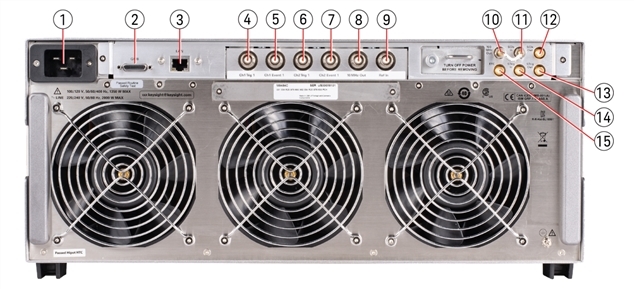
|
Item |
Connector Type
|
Description
|
|
|
# |
Name |
||
|
1 |
Line |
3-prong plug |
AC power receptacle, accepts 3-pronged AC power cord supplied with the instrument. |
|
2 |
GPIB |
Micro-D-25-pin |
IEEE-488.2, 1987 with listen and talk Use accessory: Y1260A for GPIB cabling |
|
3 |
LAN |
RJ-45 |
GbE 10/100/1000BASE-T Ethernet: the LAN supports DHCP, connection monitoring, dynamic hostname services, TCP/IP communication, TCP keep alive, and SCPI remote programming |
|
4 |
Ch1 Trig 1 |
BNC |
Channel 1 Trigger 1 input/output: 1 MΩ input impedance Threshold is adjustable from 0 V to 3.3 V Output: VOL < 0.4 V, VOH is 2.8 V to 3.3 V into high impedance 50 Ω impedance (nominal) Damage level is outside of -0.5 V to 3.8 V |
|
5 |
Ch1 Event 1 |
BNC |
Channel 1 Baseband Waveform Marker Output #1 Maximum Edge Rate: every 1.667 ns VOL < 0.4 V, VOH is 2.8 V to 3.3 V into high impedance 50 Ω impedance (nominal) Damage level is outside of -0.5 V to 3.8 V |
|
6 |
Ch2 Trig 1 |
BNC |
Channel 2 Trigger 1 input/output: (not used for a single channel instrument) 1 MΩ impedance Threshold is adjustable from 0 V to 3.3 V Output: VOL < 0.4 V, VOH is 2.8 V to 3.3 V into high impedance 50 Ω impedance (nominal) Damage level is outside of -0.5 V to 3.8 V |
|
7 |
Ch2 Event 1 |
BNC |
Channel 2 Baseband Waveform Marker Output #2 Maximum Edge Rate: every 1.667 ns (not used for a single channel instrument) VOL < 0.4 V, VOH is 2.8 V to 3.3 V into high impedance 50 Ω impedance (nominal) Damage level is outside of -0.5 V to 3.8 V |
|
8 |
10 MHz Out |
BNC |
Output of 10 MHz frequency reference, this port is always on +15 dBm (nominal) 50 Ω impedance (nominal) ESD damage level is 30 V |
|
9 |
Ref In |
BNC |
Externally supplied 1 MHz to 110 MHz, or 1 PPS, frequency reference, switched by the user interface; off by default. See Instrument Settings > Reference > Reference Source Input level -3 dBm to +20 dBm (nominal), 50 Ω impedance. |
|
10 |
100 MHz Outa |
SMA |
Output of 100 MHz frequency reference to be connected to SClk In. This port is always on and its output level is +15 dBm (nominal). If alternate SCLK In is provided this port should be terminated with 50 Ω load. Ports 10 and 11 are connected via a jumper at the factory. |
|
11 |
SClk Ina |
SMA |
Synchronization clock input. See Basic Sync Cabling Setup for Multi-Instrument 50 Ω impedance. +2 dBm to +12 dBm |
|
12 |
SClk Out |
SMA |
Synchronization clock output. See Basic Sync Cabling Setup for Multi-Instrument 50 Ω impedance. +2 dBm nominal |
|
13 |
STrig Out |
SMA |
Synchronization trigger input/output. To be connected to downstream STrig In for synchronization. Input: Threshold is adjustable from 0 V to 3.3 V 1 MΩ impedance Output: VOL < 0.4 V, VOH is 2.8 V to 3.3 V into high impedance 50 Ω impedance (nominal) Damage level is outside of -0.5 V to 3.8 V |
|
14 |
STrig In |
SMA |
Synchronization trigger input/output. To be connected to upstream STrig Out for synchronization. Input: Threshold is adjustable from 0 V to 3.3 V 1 MΩ impedance Output: VOL < 0.4 V, VOH is 2.8 V to 3.3 V into high impedance 50 Ω impedance (nominal) Damage level is outside of -0.5 V to 3.8 V |
|
15 |
EFC |
SMA |
Reserved for future use. ESD damage level is 30 V |
The SClk In and 100 MHz Out ports are designed for phase coherent operation between one or more M9484C VXG signal generators with Option SNC. The SClk In port should only be used to connect to upstream SClk Out from other VXGs. Keysight Technologies recommends that you do not connect any other signals to the SClk In port as the instrument specifications will not be covered by the warranty.
Jumper removal and connection should be performed when the VXG is powered off.
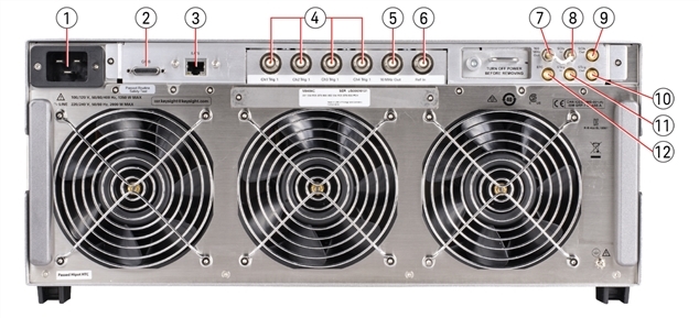
|
Item |
Connector Type
|
Description
|
|
|
# |
Name |
||
|
1 |
Line |
3-prong plug |
AC power receptacle, accepts 3-pronged AC power cord supplied with the instrument. |
|
2 |
GPIB |
Micro-D-25-pin |
IEEE-488.2, 1987 with listen and talk Use accessory: Y1260A for GPIB cabling |
|
3 |
LAN |
RJ-45 |
GbE 10/100/1000BASE-T Ethernet: the LAN supports DHCP, connection monitoring, dynamic hostname services, TCP/IP communication, TCP keep alive, and SCPI remote programming |
|
4 |
Ch1 Trig 1, Ch2 Trig 1, Ch3 Trig 1, and Ch4 Trig 1 |
BNC |
Channel 1, 2, 3, or 4 Trigger 1 input/output: 1 MΩ input impedance Threshold is adjustable from 0 V to 3.3 V Output: VOL < 0.4 V, VOH is 2.8 V to 3.3 V into high impedance 50 Ω impedance (nominal) Damage level is outside of -0.5 V to 3.8 V |
|
5 |
10 MHz Out |
BNC |
Output of 10 MHz frequency reference, this port is always on +15 dBm (nominal) 50 Ω impedance (nominal) ESD damage level is 30 V |
|
6 |
Ref In |
BNC |
Externally supplied 1 MHz to 110 MHz, or 1 PPS, frequency reference, switched by the user interface; off by default. See Instrument Settings > Reference > Reference Source Input level -3 dBm to +20 dBm (nominal), 50 Ω impedance. |
|
7 |
100 MHz Outa |
SMA |
Output of 100 MHz frequency reference to be connected to SClk IN. This port is always on and its output level is +15 dBm (nominal). If alternate SCLK In is provided this port should be terminated with 50 Ω load. Ports 7 and 8 are connected via a jumper at the factory. |
|
8 |
SClk Ina |
SMA |
Synchronization clock input. See Basic Sync Cabling Setup for Multi-Instrument 50 Ω impedance. +2 dBm to +12 dBm |
|
9 |
SClk Out |
SMA |
Synchronization clock output. See Basic Sync Cabling Setup for Multi-Instrument 50 Ω impedance. +2 dBm nominal |
|
10 |
STrig Out |
SMA |
Synchronization trigger input/output. To be connected to downstream STrig In for synchronization. Input: Threshold is adjustable from 0 V to 3.3 V 1 MΩ impedance Output: VOL < 0.4 V, VOH is 2.8 V to 3.3 V into high impedance 50 Ω impedance (nominal) Damage level is outside of -0.5 V to 3.8 V |
|
11 |
STrig In |
SMA |
Synchronization trigger input/output. To be connected to upstream STrig Out for synchronization. Input: Threshold is adjustable from 0 V to 3.3 V 1 MΩ impedance Output: VOL < 0.4 V, VOH is 2.8 V to 3.3 V into high impedance 50 Ω impedance (nominal) Damage level is outside of -0.5 V to 3.8 V |
|
12 |
EFC |
SMA |
Reserved for future use. ESD damage level is 30 V |
The SClk In and 100 MHz Out ports are designed for phase coherent operation between one or more M9484C VXG signal generators with Option SNC. The SClk In port should only be used to connect to upstream SClk Out from other VXGs. Keysight Technologies recommends that you do not connect any other signals to the SClk In port as the instrument specifications will not be covered by the warranty.
Jumper removal and connection should be performed when the VXG is powered off.